Popular Articles
3 μm CNC Precision + Constant Climate Workshop: How to Deliver “Zero-Deformation” Substrates for CVD
2026-09-21

【Core Summary】
Stable multi-run lifetime of a CVD coating rests on two things: atomic-level purity that holds metal and particle contamination down, and CTE plus interface design that survives repeated thermal cycles. A clean purity report does not equal thermal-shock readiness—geometry, ramp rates and batch traceability must be checked together.
For the full coating product line, see CVD Coating Solutions.
Core takeaway: Metal and particle contamination directly raise wafer defect and device leakage risk. Coatings are among the largest surface-area parts in the thermal field; surface and bulk impurities must be stated with GDMS/SIMS—not only by “looking dense.”

A common field scene: the supplier provides a “high-purity” report, yet the customer still sees abnormal particles or metals. The issue is often not “whether a report exists,” but detection limits, sampling locations and batch traceability.
Pushing coating purity into the <5 ppm range is mainly to keep metal contamination and particle sources controllable. For SiC and TaC coatings, excess Fe, Ni, Na or K can migrate toward the wafer at high temperature—mild cases affect epi electrical properties; severe cases create particle defects. Internally we rely primarily on GDMS, with SIMS depth profiles for critical elements, and we bind reports to coating batch numbers so customers can match incoming lots.
One line we keep repeating: a purity report is a floor, not a passport. Report pass only means the lot cleared the listed tests—it does not prove thermal cycling, geometry and process window are matched.
For temperature–atmosphere selection before purity details, see CVD SiC vs TaC Coating Selection Guide.
Core takeaway: Graphite and SiC/TaC will never have identical CTE. The engineering goal is to keep peak stress within what the coating can tolerate—via transition layers, thickness window and substrate machining precision designed together.
When micro-cracks or local spalling appear after thermal cycling, many engineers first say “coating quality is poor.” After enough failure parts, we more often see large substrate dimensional scatter, undersized corner radii, or overly steep temperature ramps stacked together.
CTE matching is not making two materials expand the same way—that is not realistic. In practice we buffer interface stress with transition layers, hold coating thickness in a sensible window, and control substrate corner R and dimensional tolerances. No matter how pure the coating is, uncontrolled interface stress still causes delamination.
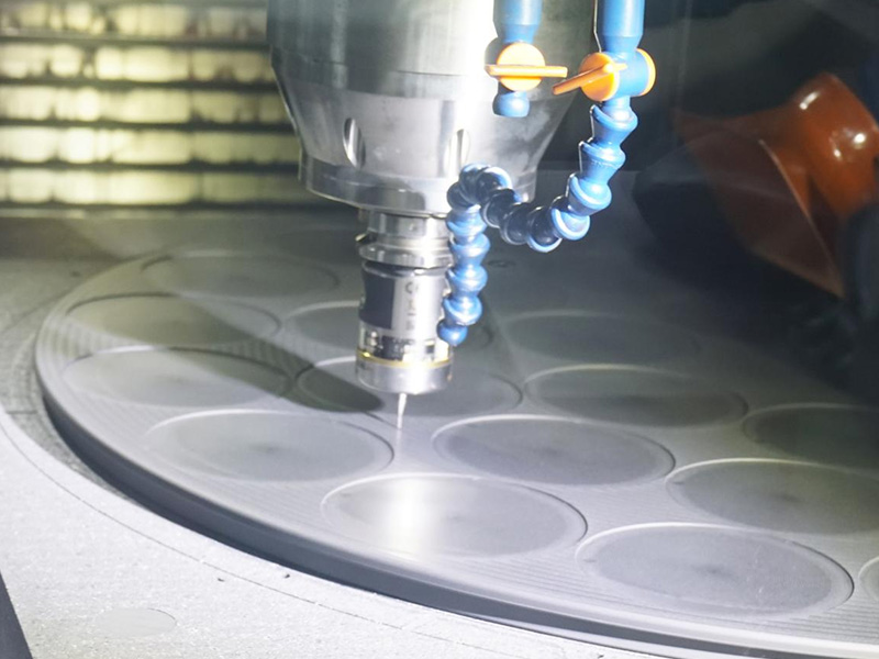
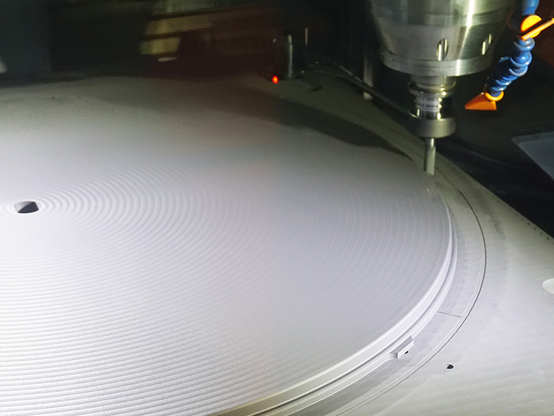
How substrate precision supports coating uniformity is covered in CNC Precision & Coating Uniformity.
Core takeaway: Check detection limits, actual values and whether the report is batch-traceable. “Typical values” without a batch report carry higher risk.
Many engineers only glance at how many “ND” appear. Three items matter more:
• Is the detection limit below the impurity levels you care about? If the limit is 10 ppm and the report says ND, that only means <10 ppm—not <1 ppm.
• Does the report map to a specific coating batch and date? Reports without batch numbers have limited value.
• Are key metals and nitrogen given as clear numbers? “ND” without a stated detection limit leaves the statement incomplete.
When we verify purity for customers, we read GDMS results together with SIMS depth profiles. A clean surface does not mean a clean bulk; a clean bulk does not mean the interface has no enrichment. Traceability is what allows a problem to be traced to a root cause—without batch linkage, the team is left guessing.
For sample characterization and failure analysis support, see Sample Mapping.
Core takeaway: A passing purity report does not guarantee thermal-shock survival. Geometry, ramp rate and material reports must sit on the same checklist—or particle shedding will recur.
An MOCVD customer reported that a new lot of CVD SiC coated susceptors passed GDMS and thickness uniformity, with normal particles on the first run. After about 20 thermal cycles, fine particles began shedding from some susceptor edges and particle counts rose. The customer suspected lot degradation.
We retested retained samples from that lot—purity and thickness remained in specification. Cross-sections of failed parts showed overall adhesion still acceptable, but stress-concentration cracks at undersized corner radii. Process records showed corner R controlled toward the lower limit on that substrate batch, and the customer’s temperature ramp was steeper than during validation. Desensitized data:
| Item | Failed lot | After adjustment |
| Particle shedding onset | ~20 cycles | No shedding over 50 continuous cycles |
| Particle count (desensitized) | From <10 /wafer to 30–50 /wafer | Back to normal range |
| Substrate corner R | Toward lower limit (~0.3 mm) | Tightened to ≥0.5 mm |
| Temperature ramp | ~15 °C/min | Recommended ≤8 °C/min |
After discussion, subsequent lots tightened corner R and substrate dimensional tolerances, and we issued ramp recommendations for that process window. Shedding stopped. The value of the case was not only fixing one shipment, but placing purity, geometry and ramp curve on the same incoming-and-process checklist for the customer.
For materials and design support on CTE and thickness windows, see Materials & Design.
Core takeaway: Purity sets the contamination floor; CTE and interface set thermal-cycle life; GDMS enables batch traceability; thermal-cycle tests check process fit. These four cannot substitute for each other.
A: Purity manages contamination and particle floor; CTE and interface manage whether the coating cracks or sheds after repeated cycles. Different problems—neither replaces the other.
A: Match the real process upper temperature, atmosphere and ramp rates as closely as possible, and define inspection points for morphology and particles. Running a meaningful fraction of design lifetime is more useful than room-temperature appearance alone.
A: No. Also check detection limits, actual values, sampling location and batch traceability. Typical values without a batch report carry higher risk.
A: Run a same-condition small-batch comparison with the same metrology—GDMS, thickness, post-cycle morphology and particles—for a meaningful number of runs before concluding. SemiXLab supports sample mapping and comparison validation.
A: Three items first: GDMS batch report, substrate corner R and dimensional tolerances, and whether thermal-cycle validation conditions are consistent. If these three do not line up, lot changes tend to introduce variation.
Core takeaway: Long CVD coating lifetime is not guaranteed by a single metric. It is the combined result of purity, CTE matching, geometric machining and thermal-cycle validation. SemiXLab’s MAE team provides full engineering support from GDMS/SIMS verification and sample mapping to failure analysis.
At SemiXLab we prefer to look at real parts, align on data and adjust parameters with customers. Coating lifetime is not secured by one report—it is managed jointly through purity, CTE, geometry and process window. If you are dealing with particles, delamination or thermal-cycle cracking, send us the process conditions and failed parts. We start with GDMS/SIMS and cross-section analysis, then provide selection and thermal-cycle validation recommendations.
Website: https://www.semixlab.com/
Technical consultation: contact the SemiXLab MAE team via the website. Free sample mapping and failure analysis requests are welcome.
1. ASTM C1282-17: Standard Test Method for Determining Chemical Durability and Etch Rate of CVD Coatings in Reactive Gas Atmospheres.
2. ASTM C1611/C1611M-21: Standard Test Method for High-Temperature Gas Corrosion and Kinetic Reaction of Advanced Ceramics.
3. ISO 20507:2014: Fine ceramics (advanced ceramics, advanced technical ceramics) — Vocabulary and Corrosion Kinetics.
4. SEMI C3-0314: Specifications for Hydrogen (H2) and Hydrogen Chloride (HCl) Gas Quality Used in Semiconductor Processing.
5. ISO 17082:2018: Advanced technical ceramics — Determination of degradation rate of ultra-high temperature ceramic (UHTC) coatings under aggressive gas environments.
About the Author
SemiXLab MAE Team (Materials & Application Engineering)
Core team members come from the Chinese Academy of Sciences system and have long experience in carbon-based materials, CVD coatings and semiconductor thermal fields. The company currently operates 12 continuous production lines. We prefer to look at real parts, align on data and adjust parameters together with customers.