Popular Articles
3 μm CNC Precision + Constant Climate Workshop: How to Deliver “Zero-Deformation” Substrates for CVD
2026-09-21

【Core Summary】
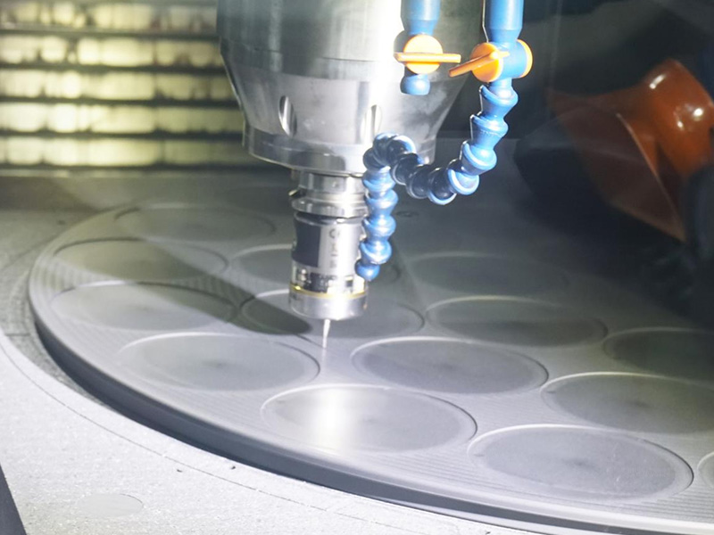
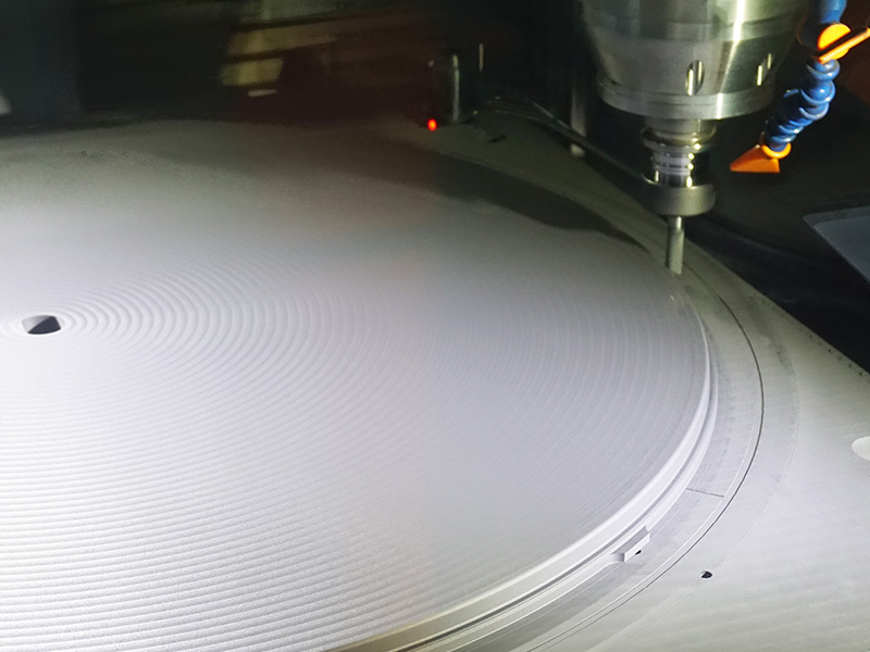
Uneven coating thickness, poor edge coverage and lot-to-lot dimensional mismatch often originate not in the deposition furnace, but in the graphite substrate state before it enters the furnace. Large graphite parts are sensitive to temperature and humidity; dimensional drift feeds directly into flow fields and deposition uniformity. At SemiXLab we run machining in a year-round constant temperature and humidity environment and hold critical dimensions to the CNC 3 μm level—so CVD starts from a repeatable physical baseline.
For the overall decision framework, see the Pillar page "CVD Coatings & Ultra-High-Purity Sources: System-Level Selection".
Core takeaway: Large, complex parts show measurable dimensional change under temperature/humidity swings. Without controlled machining and storage, the “nominal size” before the furnace drifts from real geometry.
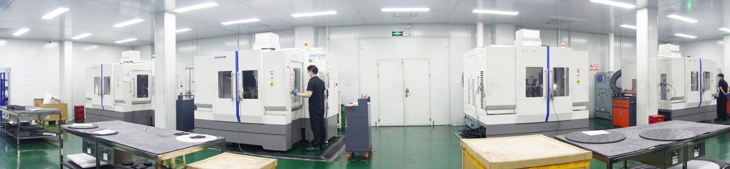
In many failure reviews, the coating recipe and the furnace did not change—only one substrate lot showed larger dimensional scatter, and thickness uniformity followed. Controlling shop climate and storage time is one of the cheapest investments in coating uniformity.
How purity and thermal-shock design link to machining is covered in "From Atomic-Level Purity to Thermal-Shock Stability".
Core takeaway: Substrate geometry tolerances affect the boundary layer and local supersaturation, which then show up as thickness and orientation variation. Without machining precision, deposition tuning cannot fully compensate for geometric error.
Corner radii, pocket depth and flatness are all “amplified” during deposition into thickness deltas or stress concentrators. Holding critical dimensions to the 3 μm level and coupling them to the coating process window gives thickness uniformity a physical foundation—instead of relying only on in-furnace parameter tweaks.
For coating products and applications, see CVD Coating Solutions.
Engineering note: An epitaxy customer reported that thickness-uniformity CPK on SiC coated susceptors fell clearly over three consecutive lots, with a slight rise in particles. Deposition recipe, gases and furnace tools were unchanged. We traced machining: two of the lots were finished during a short period in the rainy season when shop temperature/humidity briefly exceeded limits, and large parts were stored longer than the normal cycle before coating. Retained samples showed larger scatter in flatness and critical pocket dimensions. After forcing subsequent parts to be finished under constant climate and limiting storage time, thickness CPK recovered. Lesson: when coating uniformity is disputed, put the substrate’s pre-furnace dimensional state on the checklist first—do not only stare at deposition parameters.
For sample mapping and dimensional comparison of failed parts, see Sample Mapping.
Core takeaway: Too rough hurts adhesion and particles; too smooth can hurt contact in some processes. Target Ra by application window—not “the smoother the better.”
For mass-production consistency once dimensions are locked, see Mass-Production Optimization.
A: No. Prioritize mating faces, pockets and seal-related dimensions. Non-critical features balance cost and function. The point is “tighten what must be tight—and keep it stable lot to lot.”
A: Yes. SemiXLab supports customer-supplied substrates for coating, but we recommend agreeing pre-furnace dimensional and cleanliness standards; otherwise uniformity disputes are hard to attribute.
A: Review CPK or full-inspection records on critical dimensions and sample multiple lots. That is more useful than a single certificate of conformity.
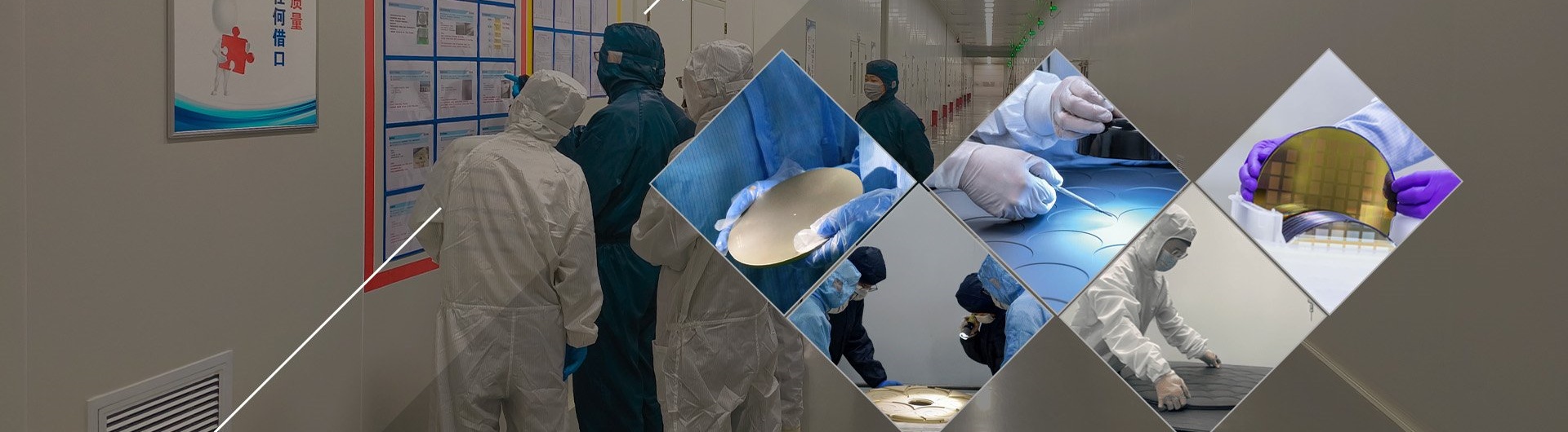
If thickness uniformity or dimensional “re-match” keeps recurring, check substrate pre-furnace state and machining environment first. If you are scaling to volume, write machining capability and the coating window into the same Copy-Exact package.
For end-to-end support from mapping to clean delivery, visit https://www.semixlab.com/ or contact the SemiXLab MAE team. Failed parts for dimensional comparison are welcome.
The next article covers the sample-to-mass-production loop: Copy-Exact, SPC and Class 100 clean logistics.
About the Author
SemiXLab MAE Team (Materials & Application Engineering)
Core team members come from the Chinese Academy of Sciences system and have long experience in carbon-based materials, CVD coatings and semiconductor thermal fields. The company currently operates 12 continuous production lines. We prefer to look at real parts, align on data and adjust parameters together with customers.