Popular Articles
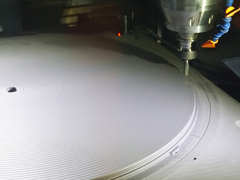
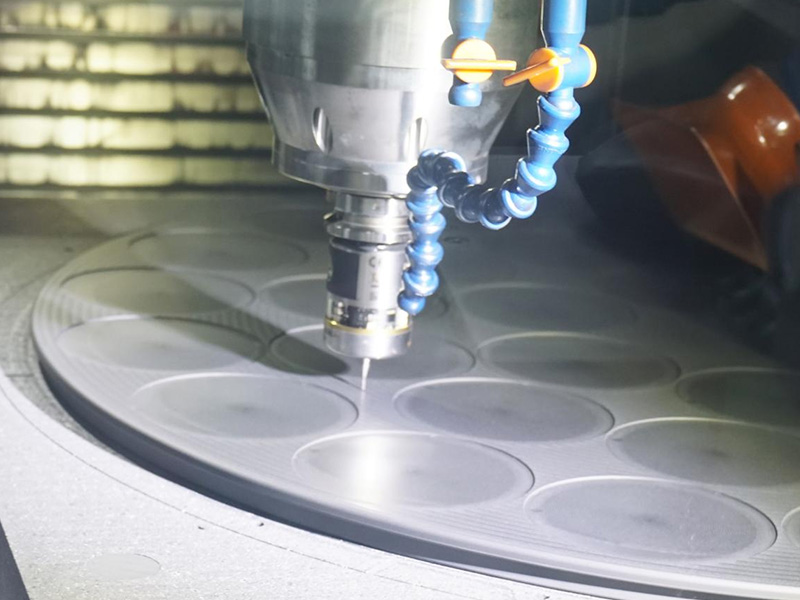
3 μm CNC Precision + Constant Climate Workshop: How to Deliver “Zero-Deformation” Substrates for CVD
2026-09-21

In SiC crystal growth, epitaxy and RTP processes, coating selection and source-material purity of thermal-field components often directly determine particle levels, crystal defects and single-furnace cost. We have distilled the questions customers ask most frequently over the past few years into five decision dimensions: how to choose the coating (SiC or TaC), how to use 7N-grade CVD-SiC source, how to balance purity with thermal-shock resistance, the impact of machining precision on coating uniformity, and how to achieve reproducible delivery from sample to volume production. This article is the overarching framework; use it to build the full picture first, then dive into each topic as needed.
I am an engineer at SemixLab. My daily work is with process colleagues at equipment makers and wafer fabs. The purpose of this article is simple—to present the pitfalls we have stepped into on the floor, the data we have validated, and the solutions that have actually been deployed, in a form engineers can use directly, rather than a pile of concepts.
Key takeaway: Looking at coating or source material alone is not enough. In a thermal-field system, the coating governs surface condition and lifetime, the source governs sublimation and defects, machining governs dimensions and uniformity, and quality control governs batch-to-batch reproducibility. When these four elements are disconnected, yield and cost of ownership (CoO) will keep fluctuating.
Many customers start by asking only “How long will this coating last?” or “What is the purity of your SiC powder?” Once the process is running, the questions become: Does the coating’s CTE match the graphite substrate? Will source particles that are too large or too small affect charging and heat transfer? If susceptor dimensions vary by tens of micrometers from batch to batch, will that affect coating-thickness uniformity? Can incoming packaging meet Class 100 requirements?
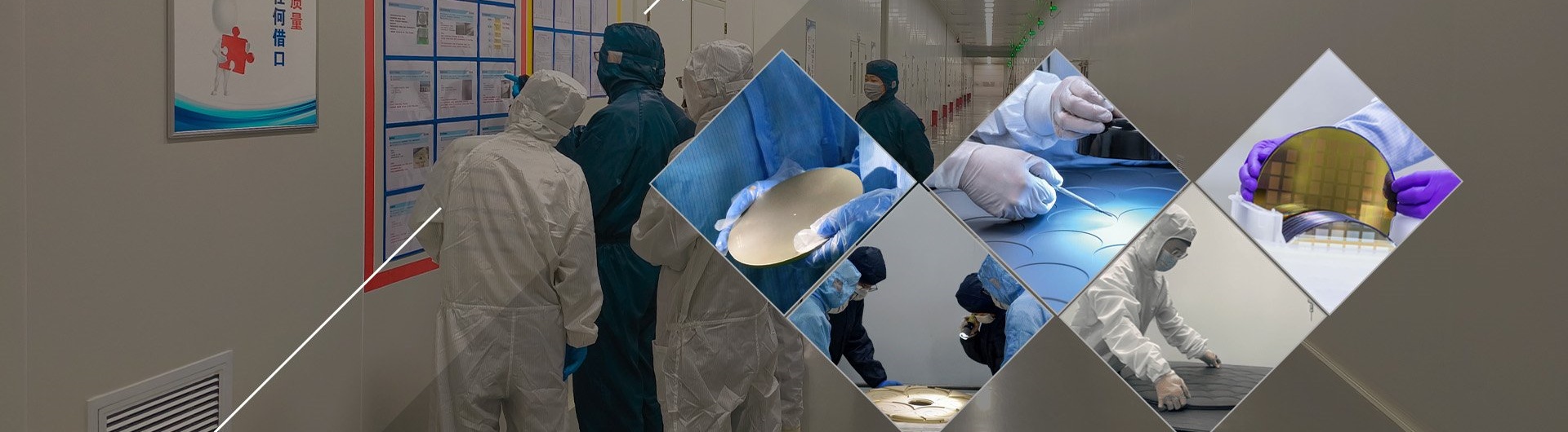
At our Zhuji base we have linked these steps into a single chain: high-purity graphite incoming inspection → climate-controlled machining (CNC accuracy to 3 μm) → CVD SiC/TaC deposition → GDMS/SIMS verification → Class 100 clean packaging. In parallel we operate an independent 7N-grade CVD-SiC source line dedicated to SiC PVT. The goal is not to sell a single product, but to enable “structural components + source material” to work together inside the same process window.
The five sub-topics that follow unpack these four links. Jump directly to the section that addresses your current bottleneck.
| Decision Dimension | Core Question | What You Get Directly |
| 1. Coating Selection | How to choose CVD SiC vs TaC by temperature, atmosphere and cost | A decision tree + application mapping for rapid SiC vs TaC judgment |
| 2. Source Optimization | How 7N-grade CVD-SiC source (N as low as 0.05 ppm) improves PVT | Concrete improvement points and experimental comparisons on impurities, carbon powder, packing density and Si/C ratio |
| 3. Purity & Reliability | <5 ppm purity + CTE matching + thermal-shock design | GDMS/SIMS verification standards, CTE-gradient design approach, thermal-cycle evaluation methods |
| 4. Precision Machining | How climate-controlled shop + CNC 3 μm safeguards coating uniformity | Environmental control, substrate tolerance, Ra vs thickness uniformity, batch CPK data |
| 5. Mass-Production Closed Loop | How Copy-Exact + SPC + Class 100 enable reproducible delivery | Mapping → first article → volume flow, rework strategy, clean logistics and system-level matching |
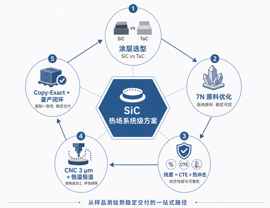
These five dimensions are not isolated. Choosing the wrong coating cannot be rescued by higher purity later; unstable machining dimensions will still cause problems in the thermal field even if the coating itself is uniform; mismatched source and thermal-field components force repeated process-window tuning. Each sub-page will explicitly note cross-links to the other dimensions for easy cross-reading.
A SiC epitaxy house experienced micro-cracking and rising particle counts after thermal cycling because of CTE mismatch between susceptor and coating, cutting component life by roughly 40 %. By switching to a matched CVD SiC coating solution and pairing it with climate-controlled CNC 3 μm precision substrate machining, lifetime returned to the design value and particle levels improved markedly. Quantified validation of this kind is routine in our daily work with customers—comparing data side-by-side and adjusting parameters together.
Key takeaway: Purity affects lifetime; machining affects uniformity; source and coating must work in concert. We separate them for clarity of explanation; in implementation they must be designed together.
A few common on-site linkage examples:
• Once coating selection is finished, immediately confirm the coating’s actual purity and thermal-shock performance under the target atmosphere (→ Purity & Reliability sub-page).
• The advantage of 7N-grade CVD-SiC source ultimately has to land on “can it run stably together with the existing thermal-field components” (→ Mass-Production Closed Loop & System Matching sub-page).
• CNC 3 μm and the climate-controlled shop are the physical foundation of coating-thickness uniformity; without that foundation, even attractive SPC charts are hard to sustain (→ Precision Machining sub-page).
• If CTE matching is poor, no amount of purity will prevent cracks and particles after thermal cycling (→ Purity & Reliability + Precision Machining sub-pages).
Key takeaway: PVT, MOCVD and RTP have different process windows and different priorities. Lock onto the most painful link for your current process, then go deep on the corresponding sub-page.
Priority focus: ultra-high-temperature stability (CVD TaC is usually required), N content and particle morphology of 7N-grade CVD-SiC source, and system matching of thermal-field components with the source. Temperatures often exceed 2000 °C; conventional SiC coatings carry higher evaporation and contamination risk. Nitrogen impurities and carbon powder on the source side translate directly into crystal defects.
Priority focus: particle control of CVD SiC coatings, CTE matching and thermal-cycle lifetime, susceptor surface roughness and thickness uniformity. Process temperatures are relatively lower, but surface cleanliness and dimensional stability requirements are extremely high—particles and metallic contamination directly hurt yield.
Priority focus: coating corrosion resistance, batch-to-batch dimensional stability of machining, and the economics of rework and re-coating. Cost and reliable repeatable supply often have to be balanced at the same time, so Copy-Exact and SPC become especially important.
Key takeaway: This page is the decision framework. Actionable details, data comparisons and cases live in the five cluster sub-pages. Enter at the point that is currently bottlenecking you rather than reading in sequence.
Recommended reading order (jump as needed):
1. Coating Selection Decision: Precision selection guide for CVD SiC vs CVD TaC under the three axes of temperature, atmosphere and cost (Sub-page 1)
2. Source Purity & Crystal-Growth Optimization: How 7N-grade CVD-SiC source systematically improves SiC PVT yield and crystal quality (Sub-page 2)
3. Purity Verification & Coating Reliability: Dual assurance from atomic-level purity to thermal-shock stability (Sub-page 3)
4. Precision Machining & Coating Uniformity: How 3 μm CNC accuracy + climate-controlled shop provide a “zero-deformation” substrate for the coating (Sub-page 4)
5. Service Closed Loop from Sample to Mass Production: How Copy-Exact + SPC + clean logistics deliver reproducible thermal-field components (Sub-page 5)
Key takeaway: Below are brief answers to the questions customers ask most often at the selection stage. Finer data, comparison tables and cases are on the corresponding sub-pages.
A: Look at the temperature window and atmosphere. For mid-to-high temperature processes such as MOCVD, epitaxy and RTP (roughly the 1400–1800 °C range), CVD SiC is preferred—mature, good thermal conductivity, relatively controllable cost. For ultra-high temperature (often >2000 °C) or strongly corrosive atmospheres such as SiC PVT, CVD TaC is the first consideration. Final choice must also factor single-furnace cost after lifetime amortization and compatibility with existing equipment. Detailed comparison is on Sub-page 1.
A: The most critical difference is nitrogen content that can be as low as ~0.05 ppm, metallic impurities held at extremely low levels, larger and more controllable particle size, and an Si/C ratio closer to 1:1. Practical effects are reduced carbon-powder introduction, higher packing density and more stable sublimation—beneficial for lowering crystal defects. See Sub-page 2 for details.
A: Large graphite parts are sensitive to temperature and humidity; dimensional drift translates directly into coating thickness and surface morphology. By controlling the machining environment and holding critical dimensional accuracy at the 3 μm level, we give subsequent CVD deposition a stable, repeatable substrate. This is the physical prerequisite for mass-production consistency. Details on Sub-page 4.
A: The standard path is sample mapping (CMM/SEM/GDMS) → material and design confirmation → first-article verification (Copy-Exact) → SPC parameter lock → volume production with Class 100 clean delivery. Non-standard geometries and rework needs can also be brought into the same workflow. Full closed loop on Sub-page 5.
A: Yes. Internally we design the two lines—“structural components + source”—in parallel. Many customers ultimately validate both inside the same process window. This reduces repeated debugging caused by interface mismatch. Concrete practice is expanded in the system-level matching section of Sub-page 5.
There is no once-and-for-all “universal coating” or “universal source” for thermal fields. What actually works is placing coating selection, source purity, machining precision and mass-production quality control inside the same framework and performing system matching against your own process window.
If you have failed parts on hand or want to validate a new process window, you are welcome to request free sample mapping or obtain a failure-analysis report. We will compare data against actual operating conditions and provide actionable recommendations.
Related products and services: CVD Coating Solutions, 7N-grade CVD-SiC Source, Sample Mapping & Mass-Production Optimization Services.
SemiXLab MAE Team (Materials & Application Engineering)
Core team members come from the Chinese Academy of Sciences system and have long been engaged in carbon-based materials, CVD coatings and semiconductor thermal-field R&D. The company was founded in 2018 and currently operates 12 continuous production lines covering the complete chain from high-purity graphite machining and CVD SiC/TaC deposition to 7N-grade CVD-SiC source synthesis. We maintain close collaboration with the Yongjiang Laboratory Thermal-Field Materials Innovation Center.
We are more accustomed to looking at physical parts, comparing data and adjusting parameters together with customers than simply sending specification sheets. If you have failed parts or wish to validate a new process window, feel free to contact us directly—we will give practical recommendations based on actual operating conditions.
Website: https://www.semixlab.com/
Brand: SemiXLab (Zhejiang Liufang Semiconductor Technology Co., Ltd.)