Popular Articles
3 μm CNC Precision + Constant Climate Workshop: How to Deliver “Zero-Deformation” Substrates for CVD
2026-09-21

Focus ring selection is not a debate over material names—“SiC versus silicon.” It centers on purity and surface roughness: the former governs metal contamination risk, while the latter drives particle adhesion and polymer behavior. For advanced nodes (3nm and below / high-aspect-ratio structures), prioritize 7N-grade CVD solid SiC. Mature nodes may start with silicon rings. This guide provides selection points and a decision matrix by the three major platforms: Lam, AMAT, and TEL.
Key takeaway: On the Lam platform, radial electric-field control by the focus ring is critical for 3D NAND and logic FinFET/GAA etch. Corrosion uniformity and surface roughness (Ra < 0.2 μm) of CVD solid SiC focus rings are core metrics for maintaining edge CD uniformity.
Lam Kiyo and Versys series operate under high-energy fluorine-based (CF₄/CHF₃) and chlorine-based (Cl₂) plasmas. Traditional single-crystal silicon focus rings exhibit higher erosion rates, shortening PM intervals. With CVD solid SiC, measured erosion rates can drop by approximately 80%, significantly extending maintenance cycles. Key parameters to prioritize during selection:
• Purity: Total metallic impurities < 0.1 ppm (7N grade) to avoid charge-related defects and heavy-metal contamination.
• Phase composition: 100% β-SiC (cubic phase), delivering isotropic etch resistance superior to single-crystal silicon.
• Density & hardness: Relative density ≥ 99.8%, Vickers hardness 28–30 GPa, strong resistance to ion bombardment.
• Surface roughness: Ra < 0.2 μm to reduce polymer adhesion and particle shedding risk.
Table 1: Key Performance Comparison of Focus Ring Materials on Lam Platform
| Performance Metric | CVD Solid SiC | Single-Crystal Si (Traditional) | Competitive Advantage |
| Chemical Purity | 99.99999% (7N) | 99.999% (5N) | Significantly lower ion-leakage risk |
| Phase Composition | 100% β-SiC | Single-crystal Si | Isotropic etch resistance |
| Relative Density | ≥99.8% (3.20 g/cm³) | — | Zero-porosity structure |
| Vickers Hardness | 28–30 GPa | ~9 GPa | Greatly improved ion-bombardment resistance |
| Surface Roughness | Ra < 0.2 μm | Ra ~0.5 μm | Less polymer adhesion |
| Fluorine-based Plasma Erosion Rate | ~80% lower | Baseline | Significantly extended PM interval |
Key takeaway: Centris multi-chamber systems demand strict thermal matching between focus rings and edge rings. The thermal conductivity and coefficient of thermal expansion of CVD solid SiC help maintain process consistency across chambers and reduce wafer-to-wafer variation caused by temperature drift.
On the Applied Materials Centris platform, the focus ring not only confines the plasma but also directly influences edge temperature distribution on the wafer. The high thermal conductivity of solid SiC enables rapid thermal equilibrium, lowering the risk of edge overheating or undercooling. Key confirmation points during selection:
• Dimensions & interfaces: Strictly match OEM drawing tolerances (typically ±0.02–0.05 mm) to ensure drop-in replacement.
• Thermal-cycling stability: Support multiple high-temperature clean and cool-down cycles without micro-cracks or delamination.
• Surface treatment: Optional precision polishing or specific roughness windows to match different polymer deposition behaviors.
Key takeaway: TEL platforms impose extremely strict particle control at advanced nodes. The zero-porosity structure and high-hardness surface of CVD solid SiC effectively reduce particle generation sources, while its plasma-erosion resistance supports longer service life.
Tokyo Electron Tactras and Vigus series demand very high chamber cleanliness in mixed logic and memory applications. As a component directly exposed to high-density plasma, the focus ring’s material purity and surface integrity directly affect defect density. At the selection stage, request from the supplier: full-element ICP-MS impurity reports, SEM surface morphology images, and accelerated lifetime test data.
Key takeaway: Selection should not merely compare “SiC vs. silicon.” Build a decision matrix around three dimensions: process window, cost model, and supply-chain reliability.
The following framework helps engineers quickly identify suitable options in real projects:
Table 2: Focus Ring / Edge Ring Selection Decision Matrix
| Decision Dimension | Prioritize CVD Solid SiC | Consider Traditional Si Rings | Recommended Action |
| Process Node | 3nm & below / HAR structures | 28nm & above mature nodes | Prioritize SiC for advanced nodes |
| Plasma Type | High-energy fluorine / chlorine | Low-power mild etch | Validate by measured erosion rate |
| Particle Sensitivity | Extremely strict defect density | Moderate particle level acceptable | Request particle performance data |
| Target Lifetime | Desire significantly longer PM cycles | Accept conventional replacement frequency | Calculate TCO comparison |
| Budget & Supply Chain | Value long-term stability & domestic control | Cost-sensitive, short-term switch | Evaluate local supply capability |
Recommendations for Dimension & Specification Selection:
1. Prioritize obtaining complete drawings of the OEM or currently used focus/edge rings. Confirm inner diameter, outer diameter, height, locating features, and electrode mating dimensions.
2. Require CNC precision control of critical mating surfaces at the ±3 μm level, and request full-dimensional inspection reports.
3. Select surface roughness according to process needs: standard recommendation Ra < 0.2 μm; certain applications requiring specific roughness to control polymer behavior can be customized.
4. For first introduction, perform small-batch installation validation (including particle testing, CD uniformity, and lifetime tracking) before scaling procurement.
Key takeaway: We are not simply a materials supplier. We are a materials technology company with full-chain capability—from high-purity raw-material synthesis and precision machining to final cleanliness and lifetime validation.
Specific capabilities include:
• High-purity CVD solid SiC: Metallic impurities controlled at sub-ppm levels; phase purity 100% β-SiC.
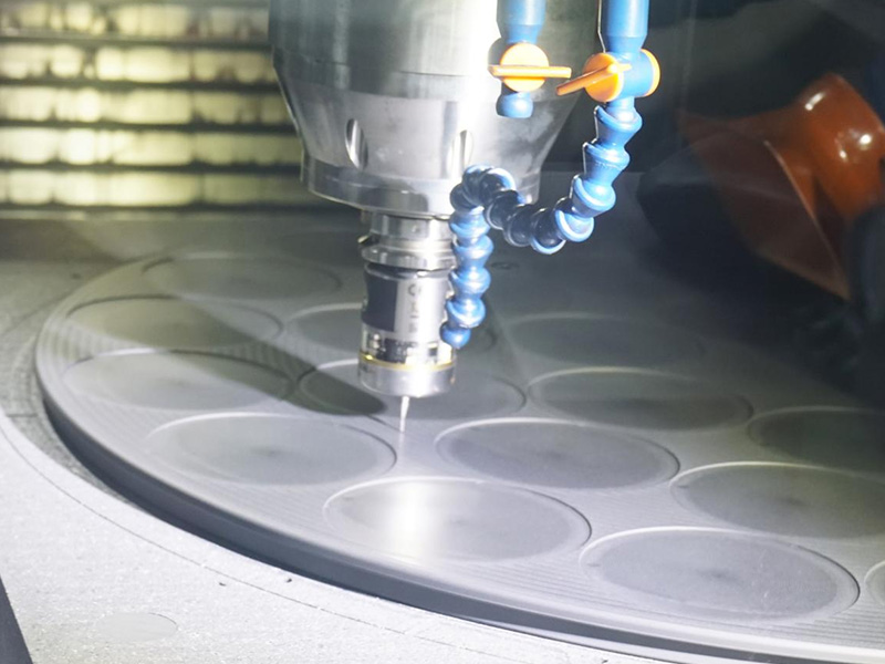
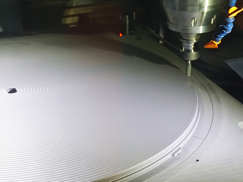
• Precision machining: CNC accuracy down to ±3 μm, supporting complex locating structures and thin-wall features.
• Surface engineering: Ultra-smooth polishing or multi-zone roughness customization to match different plasma chemistries.
• Compatibility validation: Drop-in replacement validation already covered for mainstream Lam, AMAT, and TEL tool types.
• Domestic supply chain: Full control from raw material to finished part, with advantages in delivery lead time and technical response.
Typical customer case: A domestic 12-inch logic foundry adopted Semixlab CVD solid SiC focus rings on Lam Kiyo tools. Under the same CF₄/CHF₃ process conditions, PM intervals were significantly extended and particle adders were clearly reduced (specific data desensitized per customer request).
Under typical high-energy fluorine-based plasma conditions, erosion rates can be reduced by approximately 80%. The actual extension of PM intervals depends on specific process power, gas ratios, and cleaning frequency. Most customers report maintenance cycles improved by 1.5–2.5×. We can provide accelerated lifetime evaluation tailored to your process conditions.
Dimensions and installation interfaces are designed strictly to OEM specifications of each brand, supporting drop-in replacement with no tool modification. For first introduction, we recommend baseline particle and CD-uniformity comparison validation to confirm no process-window shift.
Every batch can be supplied with full-element ICP-MS impurity reports, relative-density tests, surface-roughness inspection reports, and SEM morphology images. Key customers may arrange third-party retesting or on-site witnessing of sampling.
No hard minimum order quantity; orders can be placed according to actual needs. Standard-specification lead times are typically short. Fully customized parts (including reverse engineering) can usually complete first articles in about 2–4 weeks after drawing confirmation, depending on complexity.
In advanced-node plasma etching, focus rings and edge rings have evolved from “ordinary consumables” into critical process components that affect yield and equipment efficiency. Choosing high-purity, high-hardness, low-erosion-rate CVD solid SiC material is an effective path to balance particle control, lifetime, and total cost of ownership.
Semixlab focuses on R&D and scaled production of CVD solid SiC and complementary coating materials, with complete capability from materials synthesis to precision component delivery. If you are evaluating a focus-ring / edge-ring upgrade path, or facing process challenges related to particles and lifetime, we welcome you to contact us for technical discussion or sample verification. Please note “Etch Focus Ring Selection Inquiry” for priority response.
Semixlab is a national-level “Specialized, Refined, Distinctive, and Innovative” little-giant enterprise focused on high-purity CVD solid SiC, CVD SiC/TaC coatings, and advanced semiconductor thermal-field and chamber components. We serve global advanced-process and third-generation semiconductor customers with one-stop solutions from materials to components.Typical customers: leading domestic 12-inch logic foundries, advanced memory companies, and multiple research institutes (desensitized).
Technical Marketing Team, Semixlab. Focused on application selection and process-matching support for semiconductor chamber consumables and thermal-field materials.
— This article is a Semixlab technical selection guide for reference only. Final selection should be confirmed against actual process conditions and equipment specifications. —
Website: www.semixlab.com| For inquiries, please visit the Contact page