
-
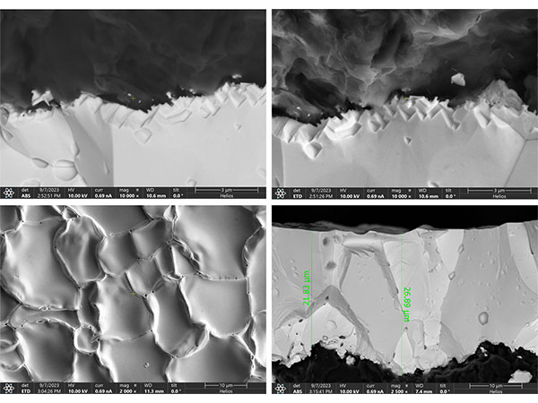
What is tantalum carbide coating used for?
2025-05-19Abstract: Tantalum Carbide (TaC) coating is a high-performance ceramic material applied to protect critical components in extreme environments, particularly in semiconductor manufacturing . We will delve into its definition, physical properties...
Read More -
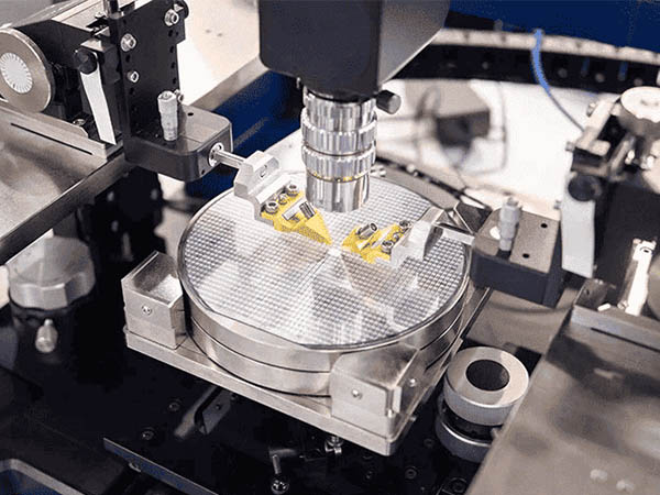
Manufacturing issues of electrostatic chuck
2025-05-12Abstract: Electrostatic chucks use electrostatic force to hold wafers on their surface and are mainly used in vacuum processes such as plasma etching. We will briefly describe the difficulties in the manufacturing process from the perspectives ...
Read More -
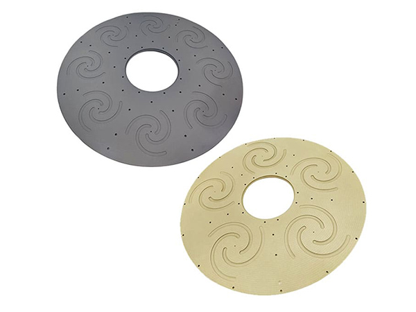
What is Silicon Carbide (SiC) Epitaxy?
2025-04-30Abstract:As the core material of next-generation power semiconductors, silicon carbide (SiC) is driving significant improvements in energy efficiency and system performance. In the SiC device manufacturing chain, silicon carbide epitaxy...
Read More -
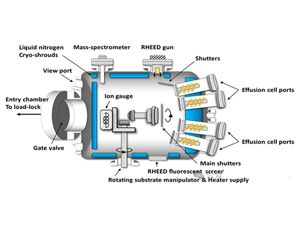
What's the difference between MBE and MOCVD?
2025-04-25Ⅰ. Common Features of MBE and MOCVDWorking Environment: Both operate in a cleanroom environment.Application Scope: Both techniques can produce identical epitaxial structures in specific material systems, such as arsenides.Ⅱ. The differences be...
Read More -
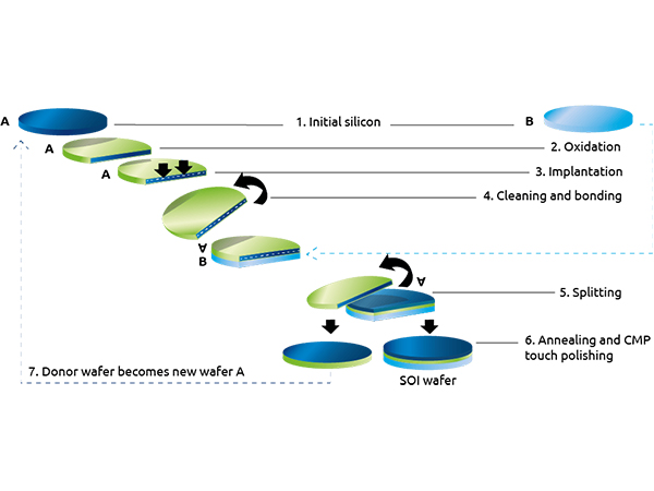
Smart Cut technology for 3C SiC wafers: Breakthrough manufacturing process and application prospects
2025-04-18Ⅰ. Technical Principles and Core AdvantagesWhat is Smart Cut technology?Smart Cut is an advanced semiconductor manufacturing process based on ion implantation and wafer splitting, specifically designed to produce ultra-thin, highly uniform ...
Read More -
What are the difference between CVD and MOCVD?
2025-04-16Chemical vapor deposition (CVD) and metal organic chemical vapor deposition (MOCVD) are both key technologies in the field of thin film deposition and are widely used in semiconductor manufacturing. However, there are significant differenc...
Read More